

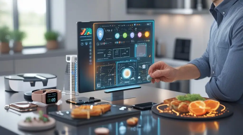
From smartwatches and smartphones to smart home devices and kitchen appliances, consumer electronics have evolved rapidly. Today, nearly every product integrates some level of connectivity. However, as devices become smaller and more powerful, design challenges increase significantly. That is exactly where electromagnetic simulation for consumer electronics design becomes essential.
At Mettler Design, advanced simulation tools like SIMULIA CST Studio Suite help engineers address these challenges early in the design cycle. As a result, manufacturers can reduce development risks, optimize performance, and accelerate time to market.
In this blog, we explore how electromagnetic simulation plays a critical role in modern consumer electronics and how Mettler Design applies these technologies to deliver efficient, reliable, and compliant products.
The Growing Complexity of Connected Consumer Electronics
Modern consumer electronics pack impressive functionality into extremely compact form factors. Devices such as smartphones, wearables, IoT sensors, and smart appliances rely on multiple wireless technologies, including:
- Cellular (4G and 5G)
- WiFi
- Bluetooth
- GPS
- NFC
At the same time, these devices are battery-powered and thermally constrained. Therefore, even small inefficiencies in antenna design, PCB layout, or electromagnetic behavior can directly impact user experience.
Shortened battery life, overheating, signal dropouts, and regulatory compliance failures are common risks. Consequently, engineers must achieve higher accuracy and tighter integration than ever before.
Why Electromagnetic Simulation Is No Longer Optional
Traditional trial-and-error prototyping methods are no longer practical for today’s complex devices. Iterative physical testing is costly, time-consuming, and often reveals issues too late in the development cycle.
Instead, electromagnetic simulation for consumer electronics design enables engineers to:
- Predict performance before manufacturing
- Optimize designs early and efficiently
- Reduce the number of physical prototypes
- Validate compliance with industry standards
At Mettler Design, simulation-driven workflows ensure that performance, reliability, and compliance are built into the product from the start.
SIMULIA CST: A One-Stop Electromagnetic Simulation Platform
SIMULIA CST Studio Suite stands out as a comprehensive solution for analyzing and optimizing electromagnetic behavior across consumer electronic devices. It supports characterization, testing, and optimization for nearly every type of electromagnetic application.
Because of its broad solver portfolio and seamless workflows, SIMULIA CST enables engineers to evaluate designs at both component and system levels.
Mettler Design leverages SIMULIA CST to deliver accurate, data-driven insights throughout the product development lifecycle.
Key Electromagnetic Elements That Require Simulation

4 Categories of PCB Electromagnetic Elements That Require Simulation
Many electromagnetic challenges originate on the printed circuit board (PCB). While PCB design tools like Altium and Cadence excel at layout, they lack full-system electromagnetic simulation capabilities.
SIMULIA CST fills this gap by importing PCB designs and analyzing their real-world electromagnetic behavior. Let’s break down the four most critical categories.
1. PCB Validation and Optimization
Importing PCB Designs into SIMULIA CST
Using SIMULIA CST PCB Studio, engineers can import fully defined PCB stack-ups directly from electronic design automation (EDA) tools. This process preserves layer definitions, materials, and geometries, enabling accurate simulation.
Once imported, Mettler Design engineers can review the stack-up, make design adjustments, and prepare the model for advanced analysis.
Signal Integrity and Power Integrity Analysis
After import, simulation workflows allow engineers to analyze:
- Signal integrity using eye diagrams
- Power integrity and voltage drop (IR analysis)
- Design rule checks (DRC)
These analyses help identify potential issues such as signal degradation, timing errors, and excessive power loss. As a result, designers can correct problems before fabrication.
System-Level PCB Analysis
Beyond trace-level analysis, SIMULIA CST allows exporting the entire board—or specific sections—into the 3D Microwave Studio. This step is crucial because it reveals how external elements like housings, enclosures, and materials affect electromagnetic performance.
At Mettler Design, this system-level approach ensures that final products perform as expected in real-world conditions.
2. Antenna Design and Placement Optimization
Designing Antennas for Compact Devices
Antenna design represents one of the most challenging aspects of modern consumer electronics. Limited space, multiple frequency bands, and close proximity to other components create complex electromagnetic interactions.
SIMULIA CST offers multiple solvers and workflows for antenna design, whether engineers are:
- Designing antennas from scratch
- Refining existing antenna models
- Importing designs from Antenna Magus
- Simulating antenna arrays and full assemblies
Evaluating Antenna Performance
Using SIMULIA CST, engineers can analyze:
- Radiation patterns
- S-parameters
- Efficiency and gain
- Coupling between antenna elements
By simulating antenna placement within the full device assembly, Mettler Design ensures optimal performance across all operating conditions.
3. Thermal Analysis for High-Density Electronics
Why Thermal Effects Matter
As consumer electronics become smaller and more powerful, heat dissipation becomes a critical concern. Higher-frequency transmission, especially in 5G and IoT devices, increases power density and thermal stress.
Without proper thermal management, devices may suffer from:
- Reduced performance
- Component degradation
- User discomfort
- Regulatory failures
Coupled Electromagnetic and Thermal Simulation
SIMULIA CST includes multiple thermal solvers that can operate independently or in a coupled electromagnetic-thermal workflow. This capability allows engineers to evaluate how electrical performance and temperature influence each other.
Mettler Design uses these simulations to:
- Analyze heat distribution in complete devices
- Evaluate passive and active cooling strategies
- Assess airflow effects on electronics
As a result, products achieve both electrical efficiency and thermal reliability.
4. EMC, EMI, and SAR Compliance
Understanding EMC and EMI Challenges
Electromagnetic compatibility (EMC) and electromagnetic interference (EMI) represent unintended electromagnetic emissions that can disrupt device performance.
For example, an unshielded microstrip trace may radiate signals that interfere with nearby components. These issues can compromise reliability and lead to compliance failures.
Simulating EMC and EMI Behavior
SIMULIA CST’s EMC/EMI solvers allow engineers to:
- Identify electromagnetic weak points
- Visualize interference paths
- Test shielding effectiveness
- Optimize spacing and grounding
At Mettler Design, these insights help prevent costly redesigns and ensure regulatory compliance.
Specific Absorbed Radiation (SAR) Analysis
For devices used close to the human body, such as smartphones and wearables, SAR compliance is critical. SIMULIA CST enables accurate SAR simulation using realistic human models.
By evaluating radiation exposure early, Mettler Design ensures products meet safety standards without sacrificing performance.
The Value of Simulation-Driven Design at Mettler Design

By integrating electromagnetic simulation for consumer electronics design into every stage of development, Mettler Design delivers measurable advantages:
- Reduced prototyping costs
- Faster development cycles
- Improved battery life and thermal performance
- Enhanced wireless connectivity
- Regulatory compliance confidence
Instead of reacting to problems late in the process, simulation enables proactive, informed decision-making.
The Bottom Line
Consumer electronics continue to evolve rapidly, becoming smaller, smarter, and more connected. However, this evolution introduces complex electromagnetic challenges that traditional design methods cannot address alone.
With SIMULIA CST Studio Suite, Mettler Design offers a powerful, one-stop solution for PCB validation, antenna optimization, thermal analysis, and EMC/EMI compliance. By leveraging advanced simulation tools, manufacturers can optimize designs before production, reduce risk, and deliver superior products to market.
If you want to enhance your consumer electronics design process and stay competitive in an increasingly connected world, Mettler Design’s simulation-driven expertise provides the clarity and confidence you need.
